Memory Basics: RAM, ROM, and Flash
Memory is where digital systems keep instructions, variables, buffers, calibration constants, logs, and firmware images. A processor without memory can compute only for an instant; a useful system needs storage at several speeds, costs, and retention levels.
Learning Objectives
By the end of this lesson, you should be able to:
- Distinguish volatile and non-volatile memory.
- Calculate capacity, address width, and data-bus width.
- Compare SRAM, DRAM, ROM, EEPROM, NOR Flash, and NAND Flash.
- Explain why memory hierarchy improves system performance.
- Identify practical issues such as refresh, endurance, wear leveling, ECC, and power-fail corruption.
Memory Fundamentals
A memory device stores binary data in addressable locations.
| Term | Meaning |
|---|---|
| Bit | One stored 0 or 1 |
| Byte | 8 bits |
| Word | Natural data width of the system, such as 16 or 32 bits |
| Address | Number used to select a location |
| Data bus | Wires that carry the value being read or written |
| Access time | Delay from valid address/control to valid data |
| Retention | How long data remains valid |
Memory is commonly described as:
$$
\text{capacity} = \text{depth} \times \text{width}
$$
If a memory has 2^N locations, it needs N address lines:
$$
N_{address} = \log_2(\text{number of locations})
$$
Example: a 64K x 8 memory has 65,536 locations, each 8 bits wide. It stores 65,536 bytes = 64 KiB and needs 16 address lines because 2^16 = 65,536.
Volatile and Non-Volatile Memory
Volatile memory loses data when power is removed. Non-volatile memory retains data without power, but writes are usually slower and have finite endurance.
Basic Memory Interface

A parallel memory interface usually has:
- Address pins
A0...Anto select a location. - Data pins
D0...Dmto transfer the value. - Chip select
CS#to enable the device. - Output enable
OE#to drive read data. - Write enable
WE#to store write data.
Read operation:
- Put a valid address on the address pins.
- Assert
CS#. - Deassert
WE#and assertOE#. - Wait at least the specified access time.
- Sample the data pins.
Write operation:
- Put a valid address on the address pins.
- Drive the write value on the data pins.
- Assert
CS#andWE#for the required pulse width. - Hold address and data stable for the datasheet hold time.

SRAM: Static RAM
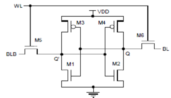
SRAM stores each bit in a latch, commonly a six-transistor cell. As long as power remains valid, the cell keeps its state without refresh.
| Property | SRAM |
|---|---|
| Volatile | Yes |
| Typical access | Very fast, often 1 ns to tens of ns |
| Density | Lower than DRAM |
| Interface | Simple |
| Refresh | Not required |
| Cost per bit | High |
SRAM is used for CPU cache, microcontroller RAM, FPGA block RAM, FIFOs, small frame buffers, and high-speed packet buffers.
DRAM: Dynamic RAM
DRAM stores each bit as charge on a capacitor controlled by an access transistor.
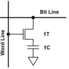
That capacitor leaks, so DRAM must be refreshed periodically. Reads are also destructive internally: the sense amplifier reads the tiny charge difference and then restores the cell.
| Property | DRAM |
|---|---|
| Volatile | Yes |
| Typical access | Slower latency than SRAM, high burst bandwidth |
| Density | High |
| Interface | Needs memory controller |
| Refresh | Required, commonly all rows within about 64 ms |
| Cost per bit | Low |
Modern SDRAM and DDR memories transfer data in bursts synchronized to a clock. DDR means double data rate: data transfers occur on both rising and falling clock edges.
ROM, PROM, EPROM, and EEPROM
Mask ROM is programmed during manufacturing and cannot be changed later. It is reliable and economical at high volume but inflexible.
PROM can be programmed once after manufacturing. EPROM can be erased using ultraviolet light through a quartz window. EEPROM can be electrically erased and programmed, often byte by byte.
EEPROM is common in embedded systems for small values:
- Calibration constants.
- Serial numbers and MAC addresses.
- User settings.
- Last-known state.
- Small event counters.
Typical serial EEPROMs such as the 24Cxx family use I2C. They are easy to connect, but writes are slow compared with RAM and endurance is finite.
Flash Memory
Flash memory is electrically erasable non-volatile memory. It writes in pages and erases in blocks, so software must respect the erase-before-write rule.
| Feature | NOR Flash | NAND Flash |
|---|---|---|
| Best use | Code storage and execute-in-place | Bulk storage |
| Random read | Excellent | Page based |
| Density | Lower | Very high |
| Cost per bit | Higher | Lower |
| Interface | Parallel, SPI, QSPI, Octal SPI | Raw NAND, eMMC, UFS, SSD |
| Typical examples | MCU program Flash, boot ROM replacement | SD cards, SSDs, phones |
Flash cells wear out after a limited number of program/erase cycles. The exact value depends on technology:
| Cell Type | Bits per Cell | Endurance Trend | Common Use |
|---|---|---|---|
| SLC | 1 | Highest | Industrial and high reliability |
| MLC | 2 | Medium | Enterprise and older consumer storage |
| TLC | 3 | Lower | Consumer SSDs and cards |
| QLC | 4 | Lowest | High-capacity storage |
For frequent writes, use wear leveling. Instead of rewriting one physical block repeatedly, rotate writes across many blocks and keep metadata that points to the newest valid copy.
Memory Hierarchy
No single memory technology is fastest, largest, cheapest, and non-volatile. Systems use a hierarchy.
The higher levels are fast and small. The lower levels are slower and larger. Caches work because programs often reuse nearby instructions and data, a behavior called locality.
Embedded Memory Map Example
A small microcontroller might expose memory like this:
- Flash: example
0x0800_0000to0x0807_FFFF; NOR-like embedded Flash for program code and constants. - SRAM: example
0x2000_0000to0x2001_FFFF; working memory for stack, heap, and variables. - Peripherals: example
0x4000_0000upward; hardware registers for GPIO, UART, SPI, ADC, timers, and other blocks. - System ROM: vendor-defined boot memory that may contain a factory bootloader.
Firmware bugs often come from treating these regions as interchangeable. Flash is non-volatile but slow to erase. SRAM is fast but disappears at reset. Peripheral addresses are not memory cells; reads and writes trigger hardware behavior.
Reliability and Safety Checks
Refresh
DRAM controllers must refresh rows on schedule. A refresh failure corrupts data even when no software writes to memory.
Endurance
EEPROM and Flash have finite erase/write cycles. A data logger that writes the same address every second can destroy a location quickly unless the design rotates storage.
Power-Fail Protection
Power loss during a Flash or EEPROM write can leave data partially programmed. Use:
- CRC or checksum on stored records.
- Sequence numbers to choose the newest valid record.
- Dual-copy settings blocks.
- Journaling for larger file systems.
- Enough hold-up capacitance when a shutdown write is required.
ECC
Error-correcting code memory adds extra bits. A common server scheme corrects single-bit errors and detects many multi-bit errors. NAND Flash almost always needs ECC because raw bit errors are expected over lifetime.
Worked Examples
Address Lines
How many address lines are required for 256 KiB x 8 memory?
256 KiB = 256 x 1024 = 262,144 = 2^18 byte locations, so the device needs 18 address lines.
Data Width
A 1M x 16 SRAM has 1,048,576 locations and each location is 16 bits. Total capacity is:
Use two short steps:
$$
1,048,576 \times 16 = 16,777,216 \text{ bits}
$$
$$
16,777,216 \text{ bits} = 2 \text{ MiB}
$$
Common Mistakes
- Confusing bits and bytes when reading memory part numbers.
- Assuming Flash can overwrite
0back to1without erasing a block. - Storing high-rate logs in EEPROM without endurance calculations.
- Ignoring SRAM usage from stack, heap, DMA buffers, and interrupt handlers.
- Treating serial Flash like RAM; page program and erase latency are much slower.
- Forgetting that cache can make memory timing non-obvious in processors with data cache.
Practice
- Calculate the address lines needed for
512K x 8memory. - Calculate total capacity for a
2M x 16memory in MiB. - Choose SRAM, DRAM, EEPROM, NOR Flash, or NAND Flash for: CPU cache, boot firmware, user settings, video frame buffer, and SD card storage.
- A product writes a 32-byte setting once every minute to one EEPROM address rated for 100,000 cycles. Estimate the lifetime without wear leveling.
- Sketch a dual-copy settings record using sequence number plus CRC.
Summary
Memory design is a set of trade-offs. SRAM is fast and simple but expensive per bit. DRAM is dense and economical but needs refresh and a controller. EEPROM is convenient for small settings. NOR Flash is strong for firmware and execute-in-place. NAND Flash gives high-capacity storage but needs block management, wear leveling, and ECC.
Further Reading
- David A. Patterson and John L. Hennessy, Computer Organization and Design, memory hierarchy chapters.
- JEDEC JESD79 DDR SDRAM standards for modern DRAM terminology.
- Microchip 24AA/24LC serial EEPROM datasheets for page-write and endurance behavior.
- Winbond W25Q serial NOR Flash datasheets for erase, program, and QSPI examples.
- ONFI NAND Flash specifications for page, block, and ECC concepts.